The 555 timer is probably the most common and popular IC in hobby circuits. There are plenty of projects that use the 555 in various ways, and it's easy to find schematics to make already proven projects. However, if you are not just satisfied with using the 555 timer plug-and-play circuit, but want to understand how the 555 timer works. Then read the article and you'll know what's going on inside the 555 timer when it's working. Learn how inputs interact with supply voltages to toggle and reset outputs high and low. Find out which pins can be used to adjust the changing threshold.
How the 555 Timer Works - Learn Circuits
let's start,
· 555 Timer Internal Function Diagram
555 Timer Pinout
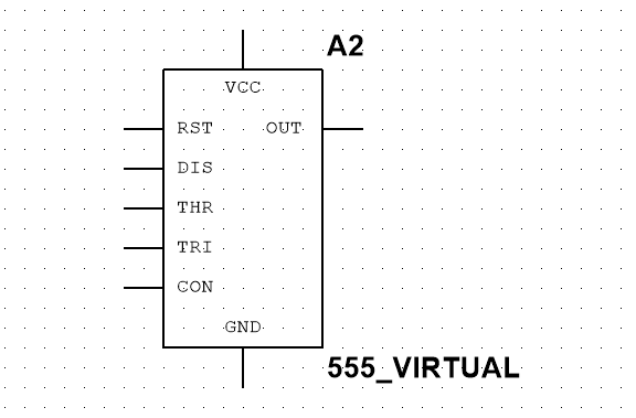
555 Timer Pinout
A 555 timer consists of eight pins
They are:
1.RST - Reset reset pin (active low)
2.DIS - Discharge triode collector Collector input pin
3.THR - Threshold upper threshold voltage pin
4.TRI - Trigger trigger pin
5.CON - Control voltage1 voltage control pin
6.OUT - Output signal output pin
7.VCC
8.GND
555 Timer Internal Function Diagram
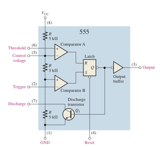
555 Timer Internal Function Diagram
The internal structure of the common 555 timer is roughly composed of the following parts
1. SR Latch
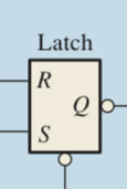
Latch Logic Symbol
Two common NOR gates internal structure of the latch:
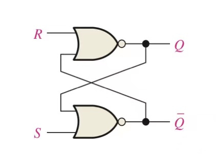
Structure 1
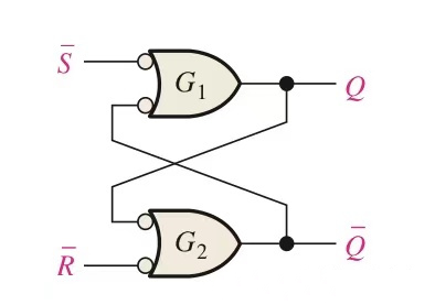
Structure 2
Two common NOR gates latches Truth Table:
For Structure 1
S Input | R Input | Q Output | Q ‾ Output |
0 | 0 | NC | NC |
0 | 1 | 0 | 1 |
1 | 0 | 1 | 0 |
1 | 1 | Invalid | Invalid |
For2 Structure 2
S ‾ Input | R ‾ Input | Q Output | Q ‾ Output |
1 | 1 | NC | NC |
1 | 0 | 0 | 1 |
0 | 1 | 1 | 0 |
0 | 0 | Invalid | Invalid |
Principle:
Input data to both ends of RS at the same time, the initial state is Q=0, Q ‾ =1. Under this condition, the judgment of the true value of the input and output is carried out along the two OR gates. (Note: the relationship between Q and Q‾true value must be opposite), and note that there cannot be a situation where S*R=1, that is, S=R=1. When this happens, for:
(1) Jump from the state S=R=0 to the state of S=R=1, because there is no independent state of S=R=1, it is necessary to judge whether to reach the state of S=0, R=1 or arrive first For the state of S=1, R=0, it is impossible to judge which of these two states, so the actual state of the SR latch cannot be macroscopically determined
(2) Jump from the state S=R=1 to the state of S=R=0, because there is no independent state of S=R=1, it is necessary to judge whether to reach the state of S=0, R=1 or arrive first For the state of S=1, R=0, it is still impossible to judge which of these two states, so the actual state of the SR latch cannot be macroscopically determined.
But for these two cases, the microscopic state is still uniquely determined. In order to avoid this situation, the constraints of the SR latch are generated:
S*R=0
Avoid the situation that the micro state cannot be uniquely determined by the macro.
2. Comparator
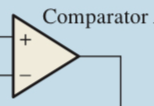
Comparator Symbol
The comparator has two input terminals, which are the positive input terminal and the negative input terminal respectively, and the input voltages are recorded as Vin+ and Vin- respectively, and the voltages of the two input terminals are compared
Input Voltage Relationship | Output terminal Vout |
Vin+>Vin- | 1 |
Vin+<Vin- | 0 |
3. NPN type semiconductor transistor (transistor)
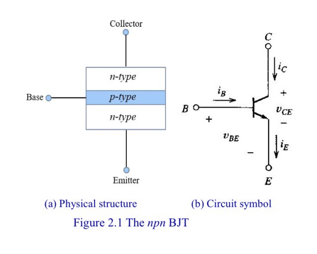
NPN type semiconductor transistor (transistor) (NPN type triode)
The content of the triode is actually quite a lot. Here is a very simple introduction to the on-off state of the triode. Taking the NPN type semiconductor triode as an example, the triode has three working states. They are:
Cut-off state: the current is cut off between the emitter and the collector, and no current flows through it
Amplified state: the current through the collector doubles with the increase of the base current (at this time, the collector and the emitter are already in a conduction state)
Saturation state: Saturation is achieved through the current on the collector, and the collector and emitter are in a fully conductive state
As shown in the figure below, it is an NPN type semiconductor triode
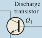
In 555 timer for
4. Filter circuit
In practical applications, it is inevitable to add decoupling capacitors to avoid the influence of noise on the trigger signal and threshold signal.
Working Principle
The overall Working principle of the 555 timer is the feedback principle
The output of a specific frequency is realized by constantly flipping the state of the triode
Take one of the wiring methods as an example
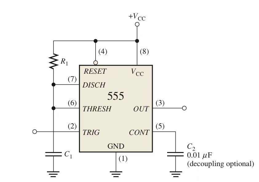
Among them, the RESET and Vcc pins are connected to a high level to make the reset pin invalid.
DIS - Discharge Transistor collector Collector input pin is connected to R1, and the divided voltage on R1 is used as the input value of the pin, and the on-off state of the triode is continuously switched according to the input value of the pin.
THR - Threshold The upper threshold voltage pin and the collector pin input act on the output level value of the comparator to the SR latch, and at the same time connect the capacitor as a charging and discharging capacitor to cause the voltage value to change
TRI - Trigger The trigger pin is waiting to be connected to other components. If it is not connected, the default input is a high level value, which acts on the output of the comparator to the SR latch.
CON - Control voltage Voltage control pin connected to decoupling capacitor stabilization circuit
GNDground
To achieve the output of a specific frequency value
The principle is as follows:
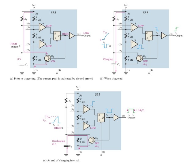
Initial state: The internal resistance of the 555 timer divides the voltage to (1/3) Vcc, and the input on the trigger pin of the initial state is high level (2) pin high level, (6) pin low level. Under the action of the comparator, it outputs a low level and acts on the SR latch at the same time. The output is Q as a low level, and then negates (you can see that there is a negation symbol-a small circle at the output). One end outputs a high level to the triode, so that the triode is in a conduction state, and Vcc flows through R1 through the triode to ground; the other end takes a non-output low level
Input a low level to the Trigger trigger pin, similar to 1. Under the action of the comparator and the latch, the node output is a low level, and the output is divided into two ends, one end makes the triode in the cut-off state, and the collector and emitter of the triode There is no current flowing between the poles, and Vcc acts on the upper plate of the capacitor from R1. As the plate is charged, the potential at the (6) pin gradually rises. When the potential at this point is greater than (2/3)Vcc, Cause the comparator to output high level, at this time (2) pin returns to low level, and the SR latch outputs high level to make the triode in the conduction state
The capacitor is charged in the process of (2.), and gradually discharges along the path shown in the figure after the triode reaches the conduction state, and returns to the (1. ) state and circulates after the discharge is completed. Every time a cycle is passed, a complete waveform is output (when the (3. ) state is reached, the state (1. ) is carried out simultaneously, and the output level value is not changed)
Note that the 555 timer in this wiring mode still needs a changing input value to be connected to the trigger pin to achieve a fixed frequency output, and to realize the "self-sufficiency" of the 555 timer, it is necessary to start from the power supply in the 555 timer. In the flat variable, the output is used as the input value of the Trigger trigger pin
The following figure realizes the "self-sufficiency" of the 555 timer:
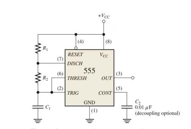
Connect to R2 to achieve voltage division
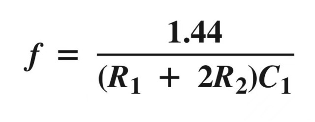
The potential of the upper plate of the capacitor is used as the input potential of the trigger pin. From the working process of the 555 timer connected only with R1, it is known that the potential on the capacitor plate will change periodically, and this period is affected by the capacitance of the capacitor and two Influenced by the resistance of resistors R1 and R2, the periodic change of the potential of the upper plate of the capacitor is taken as the input, which is equivalent to the periodic transformation process of high and low levels, and the 555 timer outputs a square wave signal with a fixed frequency.
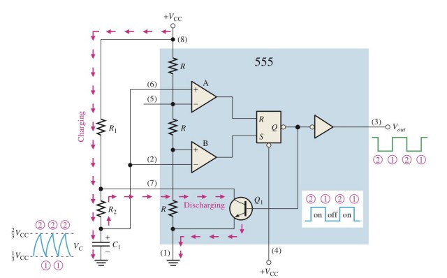
For the frequency of the output, follow the formula:
What to know more about 555 timer?
check


 Need Help?


