
Items : %s%s
SN75LVDS83BDGGR
SN75LVDS83BDGGR
FEILIDI-SN75LVDS83BDGGR
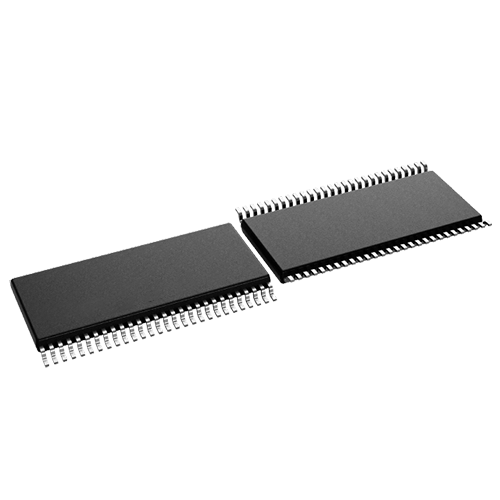
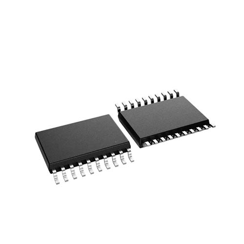
TSSOP (DGG) | 56
In Stock : 1999
Share
Please send RFQ, we will respond immediately.


Product Details
Purchasing and Inquiry
LVDS Display Series Interfaces Directly to LCD
Display Panels With Integrated LVDS
Package Options: 4.5-mm × 7-mm BGA,
and 8.1-mm × 14-mm TSSOP
1.8-V Up to 3.3-V Tolerant Data Inputs to Connect
Directly to Low-Power, Low-Voltage Application and
Graphic Processors
Transfer Rate up to 135 Mpps (Mega Pixel Per Second);
Pixel Clock Frequency Range 10 MHz to 135 MHz
Suited for Display Resolutions Ranging From HVGA
up to HD With Low EMI
Operates From a Single 3.3-V Supply and 170 mW (Typ.)
at 75 MHz
28 Data Channels Plus Clock in Low-Voltage TTL to 4
Data Channels Plus Clock Out Low-Voltage Differential
Consumes Less Than 1 mW When Disabled
Selectable Rising or Falling Clock Edge Triggered
Inputs
ESD: 5-kV HBM
Support Spread Spectrum Clocking (SSC)
Compatible with all OMAP™ 2x, OMAP™ 3x, and
DaVinci™ Application Processors
Description for the SN75LVDS83B
The SN75LVDS83B FlatLink™ transmitter contains four 7-bit parallel-load serial-out shift registers, a 7X clock synthesizer, and five Low-Voltage Differential Signaling (LVDS) line drivers in a single integrated circuit. These functions allow 28 bits of single-ended LVTTL data to be synchronously transmitted over five balanced-pair conductors for receipt by a compatible receiver, such as the SN75LVDS82 and LCD panels with integrated LVDS receiver.
When transmitting, data bits D0 through D27 are each loaded into registers upon the edge of the input clock signal (CLKIN). The rising or falling edge of the clock can be selected via the clock select (CLKSEL) pin. The frequency of CLKIN is multiplied seven times, and then used to unload the data registers in 7-bit slices and serially. The four serial streams and a phase-locked clock (CLKOUT) are then output to LVDS output drivers. The frequency of CLKOUT is the same as the input clock, CLKIN.
The SN75LVDS83B requires no external components and little or no control. The data bus appears the same at the input to the transmitter and output of the receiver with the data transmission transparent to the user(s). The only user intervention is selecting a clock rising edge by inputting a high level to CLKSEL or a falling edge with a low-level input, and the possible use of the Shutdown/Clear (SHTDN). SHTDN is an active-low input to inhibit the clock, and shut off the LVDS output drivers for lower power consumption. A low-level on this signal clears all internal registers to a low-level.
The SN75LVDS83B is characterized for operation over ambient air temperatures of –10°C to 70°C.
Alternative device option: The SN75LVDS83A (SLLS980) is an alternative to the SN75LVDS83B for clock frequency range of 10MHz-100MHz only. The SN75LVDS83A is available in the TSSOP package option only.
You can send an inquiry by email, or add the item to the RFQ list and submit it to us.
Tell us the model and quantity you need, our sales staff will reply the price in time.
 Email for receiving inquiries: jindawei@hkjdwchip.com
For your convenience, we accept multiple payment methods in USD, including PayPal, Credit Card, and wire transfer.
3. RFQ (Request for Quotations)It is recommended to request for quotations to get the latest prices and inventories about the part.
Our sales will reply to your request by email within 24 hours.
1. You'll receive an order information email in your inbox. (Please remember to check the spam folder if you didn't hear from us).
2. Since inventories and prices may fluctuate to some extent, the sales manager is going to reconfirm the order and let you know if there are any updates.
Shipping starts at $40, but some countries will exceed $40. For example (South Africa, Brazil, India, Pakistan, Israel, etc.)
The basic freight (for package ≤0.5kg or corresponding volume) depends on the time zone and country.
Currently, our products are shipped through DHL, FedEx, SF, and UPS.
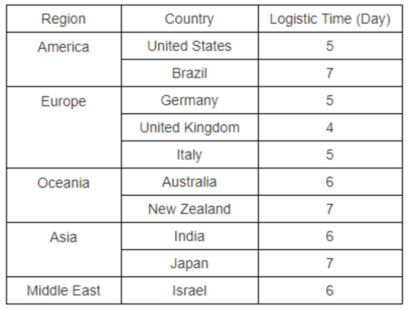
Delivery TimeOnce the goods are shipped, estimated delivery time depends on the shipping methods you chose:
FedEx International, 5-7 business days.
The following are some common countries' logistic time.
Payment Method
| The fee is charged according to the rule of PayPal. | |
| East West Bank charge US$30.00 banking fee. | |
| The fee is charged according to the rule of PayPal. | |
| Western Union charge US$0.00 banking fee. |
Shipping
| DHL(www.dhl.com) From $40.00 basic shipping fee depend on zone and country. |
|
| UPS(www.ups.com) From $40.00 basic shipping fee depend on zone and country. |
|
| FedEx(www.fedex.com) From $40.00 basic shipping fee depend on zone and country. |
|
| Registered Mail(www.singpost.com) From $10.00 basic shipping fee depend on different zone and country. |
Package
|
|
|
|
|
|
SN75LVDS83BDGGR
technical specifications, attributes, parameters and parts with similar specifications to SN75LVDS83BDGGR.
Hot Sales in Thermal
Parts with Similar Specs
The three parts on the right have similar specifications to Aavid.
-
ImagePart NameManufacturerHK JDW NOPackageStockDataSheet:Compare:
-
Texas Instruments-TCAN332DR8-SOIC (0.154, 3.90mm Width)2-3 DaysAdd Compare
-
Analog Devices Inc.feilidi-ADM3485EARZ-REEL78-SOIC2-3 DaysAdd Compare
-
Texas Instrumentsfeilidi-SN74HCS244QPWRQ120-TSSOP2-3 DaysAdd Compare
-
Artery2-5615203-2-3 Days-Add Compare
-
Tenma4685-72-7780-2-3 Days-Add Compare








 Need Help?


