

Items : %s%s


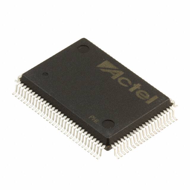
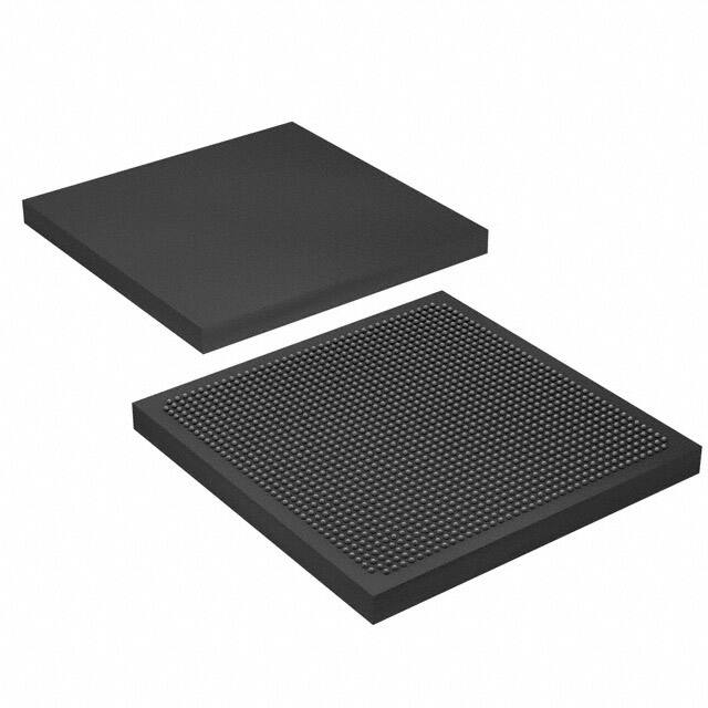
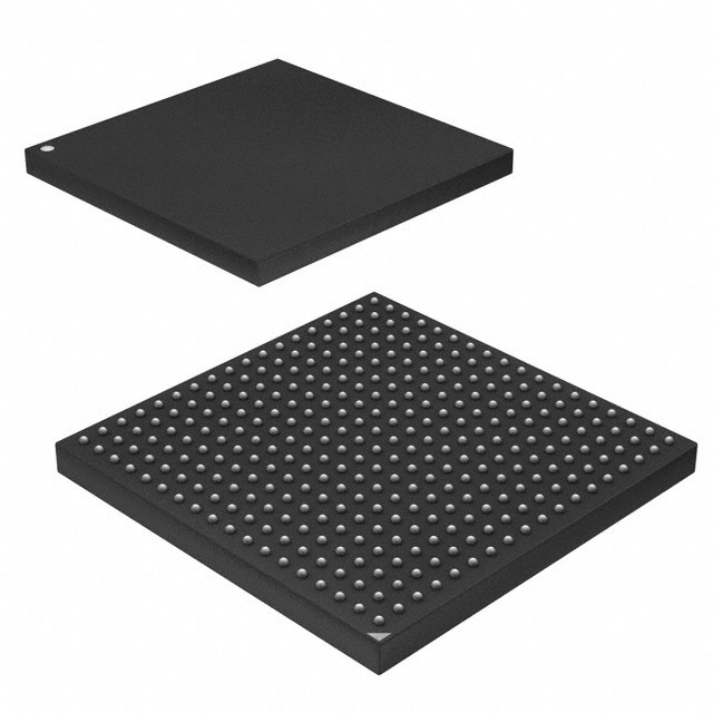
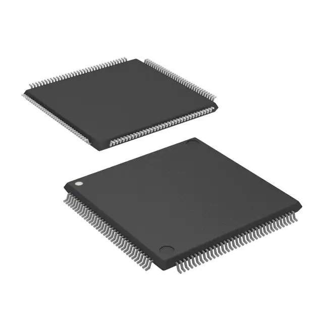
LCMXO256C-5MN100C

LCMXO256C-5MN100C
477-LCMXO256C-5MN100C
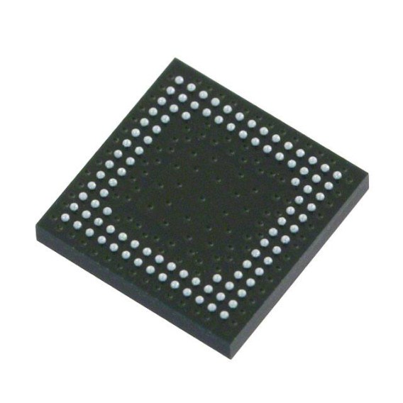
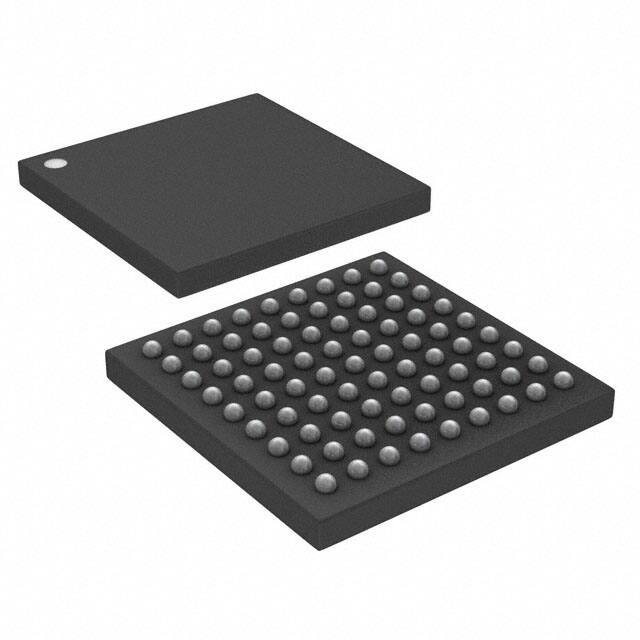
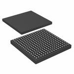
100-LFBGA, CSPBGA
3.3V V 1.35mm mm 3.5 ns ns 256B B FPGAs MachXO Series 100-LFBGA, CSPBGA 13mA mA 0.5mm mm 100
In Stock : 999
Share
Please send RFQ, we will respond immediately.


Product Details
Purchasing and Inquiry
LCMXO256C-5MN100C Overview
As part of the 100-LFBGA, CSPBGA package, it is included. The FLASH PLD-series of FPGAs are composed of this type. There are 78 I/Os for better data transfer. To form a fundamental building block, there are 256 logic elements/cells. An electrical supply voltage of 1.8V powers it. This FPGA part belongs to the family of Field Programmable Gate Arrays. An attachment Surface Mount allows the FPGA module to be attached to the development board. Fpga chips operates wFpga chipsh a supply voltage of 1.71V~3.465V. It is a type of FPGA belonging to the MachXO seies. During the operation of the system, the operating temperature should remain within the range of 0°C~85°C TJ. A total of 78 outputs are incorporated into this device. A model of this FPGA is contained in Tray for the purpose of saving space. There are a total of 100 terminations. Its base part number LCMXO256 can be used to find related parts. There is a maximum RAM si0Be of 0B on this FPGA module, which is necessary to ensure the normal operation of the program. In this case, 100 pins are used in the design. The FPGA consists of 32 LABs/CLBs. I think, as long as this FPGA is mounted in Surface Mount, it could perform excellently according to its specifications as long as you mount it in Surface Mount. When operating with the supply voltage of 3.3V, designers can fully make use of its flexibility. This device has a pin count of 100 in fpga semiconductor. In this FPGA module, there is a memory of 256B available for storing applications and data. There is a possibility that this FPGA will be able to reach a speed of 600MHz. Fpga semiconductor incorporates 256 logic cells used for the building block. Fpga semiconductor operates on 13mA of supply current. As well as being characterized by a feature called IT CAN ALSO OPERATE AT 2.5V AND 3.3V, it has another feature called A. To detect the status of input signals, there is a dedicated input which is used to detect the status of the input module. In this device, the main building blocks of a CPLD are 128 macro cells, which serve as the main components of the device. The SRAM memory is adopted for storing data and avoiding resource conflicts.
LCMXO256C-5MN100C Features
78 I/Os
100 LABs/CLBs
LCMXO256C-5MN100C Applications
There are a lot of Lattice Semiconductor Corporation LCMXO256C-5MN100C FPGAs applications.
- Wireless Communications
- Industrial IoT
- Data center hardware accelerators
- Audio
- Industrial Ethernet
- Camera time adjustments
- Electronic Warfare
- Aerospace and Defense
- Image processing
- Medical ultrasounds
You can send an inquiry by email, or add the item to the RFQ list and submit it to us.
Tell us the model and quantity you need, our sales staff will reply the price in time.
 Email for receiving inquiries: jindawei@hkjdwchip.com
For your convenience, we accept multiple payment methods in USD, including PayPal, Credit Card, and wire transfer.
3. RFQ (Request for Quotations)It is recommended to request for quotations to get the latest prices and inventories about the part.
Our sales will reply to your request by email within 24 hours.
1. You'll receive an order information email in your inbox. (Please remember to check the spam folder if you didn't hear from us).
2. Since inventories and prices may fluctuate to some extent, the sales manager is going to reconfirm the order and let you know if there are any updates.
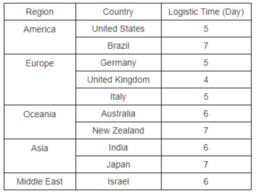
Shipping starts at $40, but some countries will exceed $40. For example (South Africa, Brazil, India, Pakistan, Israel, etc.)
The basic freight (for package ≤0.5kg or corresponding volume) depends on the time zone and country.
Currently, our products are shipped through DHL, FedEx, SF, and UPS.
Delivery TimeOnce the goods are shipped, estimated delivery time depends on the shipping methods you chose:
FedEx International, 5-7 business days.
The following are some common countries' logistic time.
Payment Method
| The fee is charged according to the rule of PayPal. | |
| East West Bank charge US$30.00 banking fee. | |
| The fee is charged according to the rule of PayPal. | |
| Western Union charge US$0.00 banking fee. |
Shipping
| DHL(www.dhl.com) From $40.00 basic shipping fee depend on zone and country. |
|
| UPS(www.ups.com) From $40.00 basic shipping fee depend on zone and country. |
|
| FedEx(www.fedex.com) From $40.00 basic shipping fee depend on zone and country. |
|
| Registered Mail(www.singpost.com) From $10.00 basic shipping fee depend on different zone and country. |
Package
|
|
|
|
|
|
LCMXO256C-5MN100C
technical specifications, attributes, parameters and parts with similar specifications to LCMXO256C-5MN100C.
Hot Sales in Thermal

.png)
Parts with Similar Specs
The three parts on the right have similar specifications to Aavid.
-
ImagePart NameManufacturerHK JDW NOPackageStockDataSheet:Compare:
-
 Lattice Semiconductor Corporation477-LCMXO2-2000HC-4TG144I144-LQFP2-3 DaysAdd Compare
 -
 Lattice Semiconductor477-LCMXO2-1200ZE-1MG132I132-LFBGA, CSPBGA2-3 DaysAdd Compare
 -
Lattice Semiconductor477-LCMXO2-256ZE-1MG132C132-LFBGA, CSPBGA2-3 DaysAdd Compare
-
Lattice Semiconductor Corporation477-LCMXO2-1200HC-4TG144I144-LQFP2-3 DaysAdd Compare
-
 Lattice Semiconductor Corporation477-LCMXO2-1200HC-4TG100C100-LQFP2-3 DaysAdd Compare
 -
Lattice Semiconductor477-LCMXO256C-3TN100I100-LQFP2-3 DaysAdd Compare
-
 Lattice Semiconductor477-LCMXO2-2000ZE-1BG256C256-LFBGA2-3 DaysAdd Compare
 -
Lattice Semiconductor477-LCMXO2-2000ZE-1BG256I256-LFBGA2-3 DaysAdd Compare
 Need Help?


